The electrical safety spacing mainly depends on the level of the plate-making factory, which is generally 0.15mm. In fact, it can be even closer. If the circuit is not related to the signal, as long as there is no short circuit and the current is sufficient, large current requires thicker wiring and spacing.
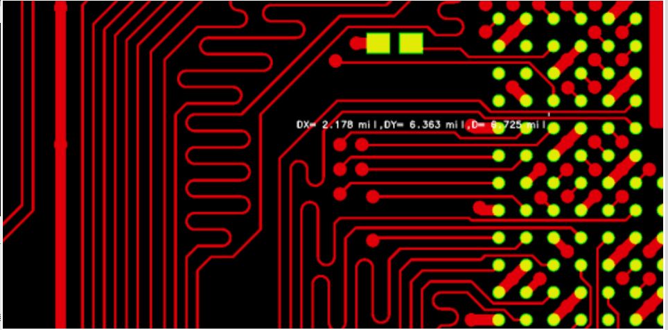
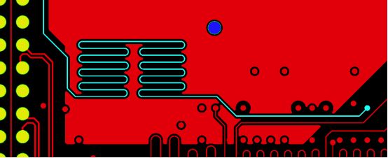
1.Distance between wires
The distance between conductors needs to be considered based on the PCB manufacturer’s manufacturing capability. It is recommended that the distance between conductors be at least 4mil. However, some factories can also produce with 3/3mil line width and line spacing. From the perspective of production, of course, the bigger the better under conditions. A normal 6mil is more conventional.
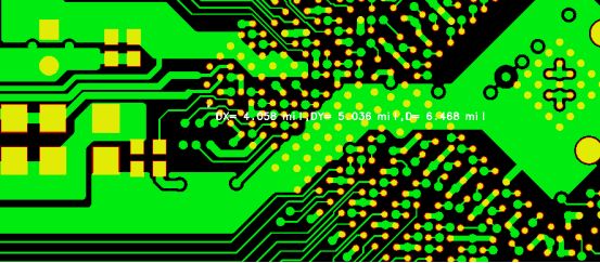
2.Spacing between pad and wire
The distance between the pad and the line is generally not less than 4mil, and the greater the distance between the pad and the line when there is space, the better. Because pad welding requires window opening, the window opening is greater than 2mil of pad. If the spacing is insufficient, it will not only cause short circuit of the line layer, but also lead to copper exposure of the line.
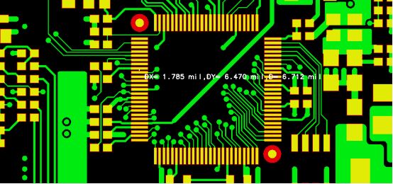
3.The spacing between Pad and Pad
The spacing between the pad and the pad should be greater than 6mil. It is difficult to make a solder stop-welding bridge with insufficient pad spacing, and the IC pad of different networks may have a short circuit when welding the open weld bridge. The distance between the network pad and the pad is small, and it is not convenient to disassemble the repaired components after the tin is fully connected on the welding.
4.Copper and copper, wire, PAD spacing
The distance between live copper skin and line and PAD is larger than that between other line layer objects, and the distance between copper skin and line and PAD is greater than 8mil to facilitate production and manufacturing. Because the size of the copper skin does not necessarily need to do much value, a little bigger and a little smaller does not matter. In order to improve the production yield of products, the spacing between the line and the PAD from the copper skin should be as large as possible.
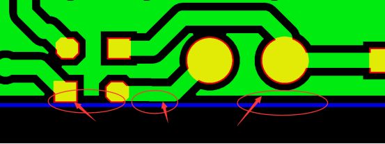
5.Spacing of wire, PAD, copper and plate edge
Generally, the distance between wiring, pad and copper skin and the contour line should be greater than 10mil, and less than 8mil will lead to copper exposure on the edge of the plate after production and molding. If the edge of the plate is V-CUT, then the spacing should be greater than 16mil. Wire and PAD are not only copper exposed so simple, line too close to the edge of the plate may be small, resulting in current carrying problems, PAD small affect welding, resulting in poor welding.`