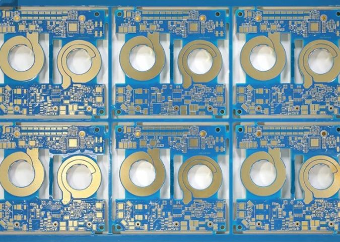
Circuit materials rely on high-quality conductors and dielectric materials to connect modern complex components to each other for optimal performance. However, as conductors, these PCB copper conductors, whether DC or mm Wave PCB boards, need anti-aging and oxidation protection. This protection can be achieved in the form of electrolysis and immersion coatings. They often provide varying degrees of weld ability, so that even with ever-smaller parts, micro-surface mount (SMT), etc., a very complete weld spot can be formed. There are a variety of coatings and surface treatments that can be used on PCB copper conductors in the industry. Understanding the characteristics and relative costs of each coating and surface treatment helps us make the appropriate choice to achieve the highest performance and longest service life of PCB boards.
The selection of a PCB final finish is not a simple process that requires consideration of the PCB’s purpose and working conditions. The current trend toward densely packed, low-pitch, high-speed PCB circuits and smaller, thinner, high-frequency PCBS poses challenges for many PCB manufacturers. PCB circuits are manufactured through laminates of various copper foil weights and thicknesses supplied to PCB manufacturers by material manufacturers, such as Rogers, who then process these laminates into various types of PCBS for use in electronics. Without some form of surface protection, the conductors on the circuit will oxidize during storage. Conductor surface treatment acts as a barrier separating the conductor from the environment. It not only protects the PCB conductor from oxidation, but also provides an interface for welding circuits and components, including lead bonding of integrated circuits (ics).
Select suitable PCB surface
Suitable surface treatment should help to meet the PCB circuit application as well as the manufacturing process. The cost varies due to different material costs, different processes and types of finishes required. Some surface treatments allow for high reliability and high isolation of densely routed circuits, while others may create unnecessary Bridges between conductors. Some surface treatments meet military and aerospace requirements, such as temperature, shock and vibration, while others do not guarantee the high reliability required for these applications. Listed below are some PCB surface treatments that can be used in circuits ranging from DC circuits to millimeter-wave bands and high speed digital (HSD) circuits:
●ENIG
●ENEPIG
●HASL
●Immersion Silver
●Immersion Tin
●LF HASL
●OSP
●Electrolytic hard gold
●Electrolytically bonded soft gold
1.ENIG
ENIG, also known as the chemical nickel-gold process, is widely used in the surface treatment of PCB board conductors. This is a relatively simple low-cost process that forms a thin layer of weldable gold on top of a nickel layer on the surface of a conductor, resulting in a flat surface with good weld ability even on densely packed circuits. Although ENIG process ensures the integrity of through-hole electroplating (PTH), it also increases the conductor loss at high frequency. This process has a long storage life, in line with RoHS standards, from the circuit manufacturer processing, to the component assembly process, as well as the final product, it can provide long-term protection for PCB conductors, so many PCB developers choose a common surface treatment.
2.ENEPIG
ENEPIG is an upgrade of the ENIG process by adding a thin palladium layer between the chemical nickel layer and the gold plating layer. The palladium layer protects the nickel layer (which protects the copper conductor), while the gold layer protects both palladium and nickel. This surface treatment is ideal for bonding devices to PCB leads and can handle multiple reflow processes. Like ENIG, ENEPIG is RoHS compliant.
3.Immersion Silver
Chemical silver sedimentation is also a non-electrolytic chemical process in which the PCB is completely immersed in a solution of silver ions to bind the silver to the surface of the copper. The resulting coating is more consistent and uniform than ENIG, but lacks the protection and durability provided by the nickel layer in ENIG. Although its surface treatment process is simpler and more cost-effective than ENIG, it is not suitable for long-term storage with circuit manufacturers.
4.Immersion Tin
Chemical tin deposition processes form a thin tin coating on a conductor surface through a multi-step process that includes cleaning, micro-etching, acid solution prepreg, immersion of non-electrolytic tin leaching solution, and final cleaning. Tin treatment can provide good protection for copper and conductors, contributing to the low loss performance of HSD circuits. Unfortunately, chemically sunk tin is not one of the longest-lasting conductor surface treatments because of the effect that tin has on copper over time (i.e., the diffusion of one metal into another reduces the long-term performance of a circuit conductor). Like chemical silver, chemical tin is a lead-free, RoHs-compliant process.
5.OSP
The organic welding protection film (OSP) is a non-metallic protective coating that is coated with a water-based solution. This finish is also RoHS compliant. However, this surface treatment does not have a long shelf life and is best used before the circuit and components are welded to the PCB. Recently, new OSP membranes have appeared on the market, which are believed to be able to provide long-term permanent protection for conductors.
6.Electrolytic hard gold
Hard gold treatment is an electrolytic process in line with the RoHS process, which can protect PCB and copper conductor from oxidation for a long time. However, due to the high cost of materials, it is also one of the most expensive surface coatings. It also has poor weldability, poor weldability for bonding soft gold treatment, and it is RoHS compliant and can provide a good surface for the device to bond to the PCB’s leads.
