Often hear “grounding is very important”, “need to strengthen the grounding design” and so on. In fact, in the PCB layout of booster DC/DC converters, grounding design without sufficient consideration and deviation from the basic rules is the root cause of the problem. Be aware that the following precautions need to be strictly followed. In addition, these considerations are not limited to booster DC/DC converters.
Ground Connection
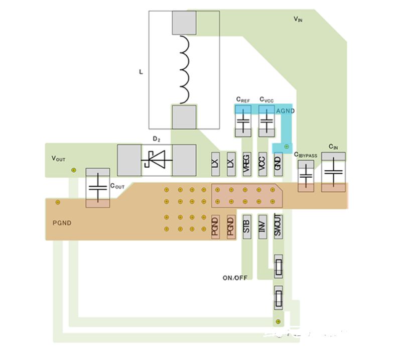
First, analog small signal grounding and power grounding must be separated. In principle, the layout of power grounding does not need to be separated from the top layer with low wiring resistance and good heat dissipation.
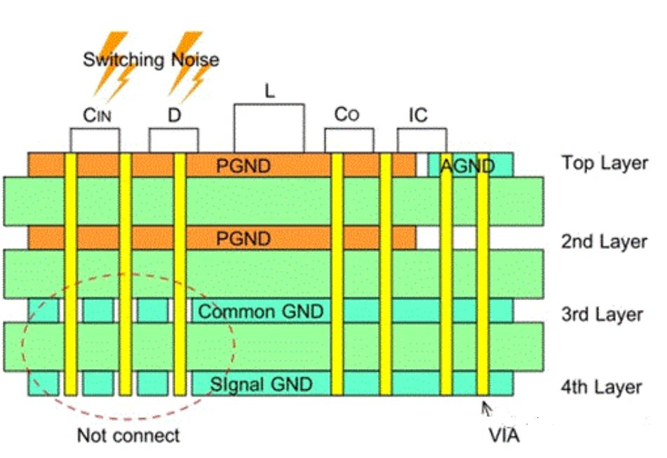
If the power grounding is separated and connected to the back through the hole, the effects of the hole resistance and inductors, losses and noise will be worsened. For shielding, heat dissipation and reducing DC loss, the practice of setting ground in the inner layer or back is only auxiliary grounding.
When the grounding layer is designed in the inner layer or back of the multilayer circuit board, special attention should be paid to the grounding of the power supply with more noise of the high-frequency switch. If the second layer has a power connection layer designed to reduce DC losses, connect the top layer to the second layer using multiple through-holes to reduce the impedance of the power source.
In addition, if there is common ground at the third layer and signal ground at the fourth layer, the connection between the power grounding and the third and fourth layers is only connected to the power grounding near the input capacitor where the high-frequency switching noise is less. Do not connect the power grounding of the noisy output or current diodes. See section diagram below.
Key Points:
1.PCB layout on the booster type DC/DC converter, the AGND and PGND need separation.
2.In principle, PGND in the PCB layout of booster DC/DC converters is configured at the top level without separation.
3.In a booster DC/DC converter PCB layout, if PGND is separated and connected on the back through the hole, loss and noise will increase due to the impact of the hole resistance and inductance.
4.In the PCB layout of the booster DC/DC converter, when the multilayer circuit board is connected to the ground in the inner layer or on the back, pay attention to the connection between the input terminal with high noise of the high-frequency switch and the PGND of the diode.
5.In the PCB layout of booster DC/DC converter, the top PGND is connected to the inner PGND through multiple through-holes to reduce impedance and DC loss
6.In the PCB layout of the booster DC/DC converter, the connection between the common ground or signal ground and PGND should be made at PGND near the output capacitor with less noise of the high-frequency switch, not at the input terminal with more noise or PGN near the diode.