Regarding the PCB layout and wiring problem, today we will not talk about signal integrity analysis (SI), electromagnetic compatibility analysis (EMC), power integrity analysis (PI). Just talking about the manufacturability analysis (DFM), the unreasonable design of manufacturability will also lead to the failure of product design.
Successful DFM in a PCB layout starts with setting design rules to account for important DFM constraints. The DFM rules shown below reflect some of the contemporary design capabilities that most manufacturers can find. Ensure that the limits set in the PCB design rules do not violate them so that most standard design restrictions can be ensured.
The DFM problem of PCB routing depends on a good PCB layout, and the routing rules can be preset, including the number of bending times of the line, the number of conduction holes, the number of steps, etc. Generally, exploratory wiring is carried out first to connect short lines quickly, and then labyrinth wiring is carried out. Global routing path optimization is carried out on the wires to be laid first, and re-wiring is tried to improve the overall effect and DFM manufacturability.
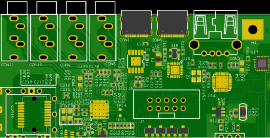
1.SMT devices
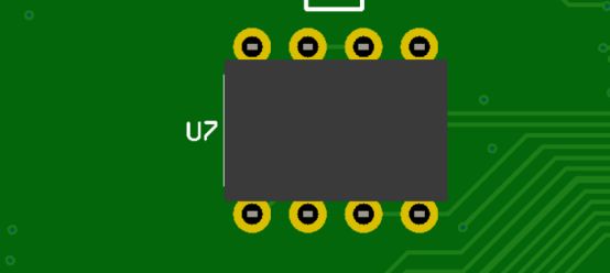
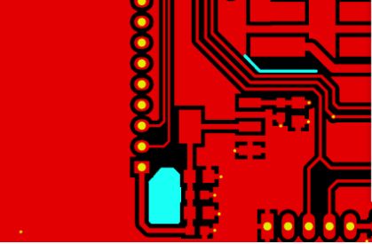
The device layout spacing meets the assembly requirements, and is generally greater than 20mil for surface mounted devices, 80mil for IC devices, and 200mi for BGA devices. In order to improve the quality and yield of the production process, the device spacing can meet the assembly requirements.
Generally, the distance between the SMD pads of the device pins should be greater than 6mil, and the fabrication capacity of the solder solder bridge is 4mil. If the distance between the SMD pads is less than 6mil and the distance between the solder window is less than 4mil, the solder bridge cannot be retained, resulting in large pieces of solder (especially between the pins) in the assembly process, which will lead to short circuit.
2.DIP device
The pin spacing, direction and spacing of the devices in the over wave soldering process should be taken into account. Insufficient pin spacing of the device will lead to soldering tin, which will lead to short circuit.
Many designers minimize the use of in-line devices (THTS) or place them on the same side of the board. However, in-line devices are often unavoidable. In the case of combination, if the in-line device is placed on the top layer and the patch device is placed on the bottom layer, in some cases, it will affect the single-side wave soldering. In this case, more expensive welding processes, such as selective welding, are used.
3.the distance between the components and the plate edge
If it is machine welding, the distance between the electronic components and the edge of the board is generally 7mm (different welding manufacturers have different requirements), but it can also be added in the PCB production process edge, so that the electronic components can be placed on the PCB board edge, as long as it is convenient for wiring.
However, when the edge of the plate is welded, it may encounter the guide rail of the machine and damage the components. The device pad at the edge of the plate will be removed in the manufacturing process. If the pad is small, the welding quality will be affected.
4.Distance of high/low devices
There are many kinds of electronic components, different shapes, and a variety of lead lines, so there are differences in the assembly method of printed boards. Good layout can not only make the machine stable performance, shock proof, reduce damage, but also can get a neat and beautiful effect inside the machine.
Small devices must be kept at a certain distance around high devices. The device distance to the device height ratio is small, there is an uneven thermal wave, which may cause the risk of poor welding or repair after welding.
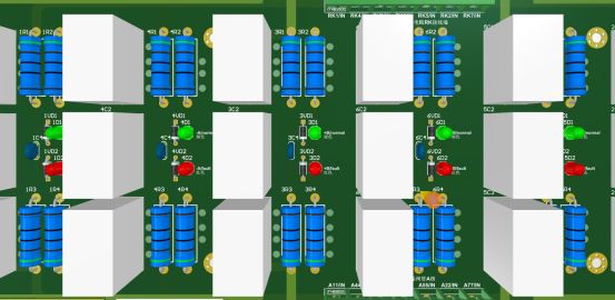
5.Device to device spacing
In general smt processing, it is necessary to take into account certain errors in the mounting of the machine, and take into account the convenience of maintenance and visual inspection. The two adjacent components should not be too close and a certain safe distance should be left.
The spacing between flake components, SOT, SOIC and flake components is 1.25mm. The spacing between flake components, SOT, SOIC and flake components is 1.25mm. 2.5mm between PLCC and flake components, SOIC and QFP. 4mm between PLCCS. When designing PLCC sockets, care should be taken to allow for the size of the PLCC socket (the PLCC pin is inside the bottom of the socket).
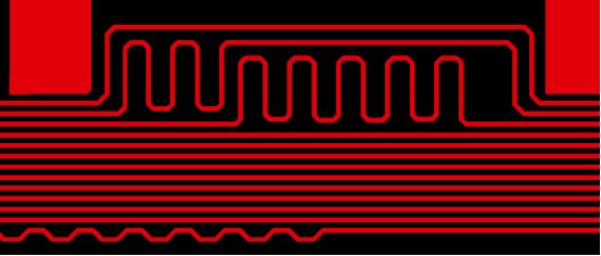
6.Line width/line distance
For designers, in the process of design, we can not only consider the accuracy and perfection of the design requirements, there is a big restriction is the production process. It is impossible for a board factory to create a new production line for the birth of a good product.
Under normal conditions, the line width of the down line is controlled to 4/4mil, and the hole is selected to be 8mil (0.2mm). Basically, more than 80% of PCB manufacturers can produce, and the production cost is the lowest. The minimum line width and line distance can be controlled to 3/3mil, and 6mil (0.15mm) can be selected through the hole. Basically, more than 70% PCB manufacturers can produce it, but the price is slightly higher than the first case, not too much higher.
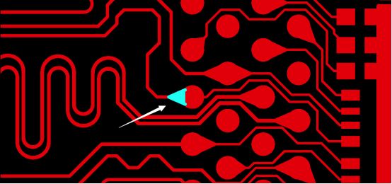
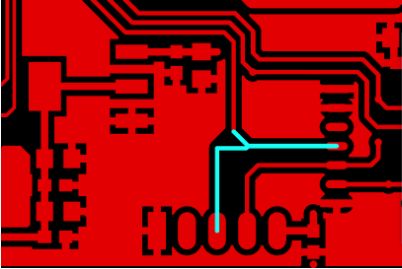
7.An acute Angle/right Angle
Sharp Angle routing is generally prohibited in the wiring, right Angle routing is generally required to avoid the situation in PCB routing, and has almost become one of the standards to measure the quality of wiring. Because the integrity of the signal is affected, the right-angle wiring will generate additional parasitic capacitance and inductance.
In the process of PCB plate-making, PCB wires intersect at an acute Angle, which will cause a problem called acid Angle. In the pcb circuit etching link, excessive corrosion of pcb circuit will be caused at the “acid Angle”, resulting in the pcb circuit virtual break problem. Therefore, PCB engineers need to avoid sharp or strange angles in the wiring, and maintain a 45 degree Angle at the corner of the wiring.
8.Copper strip/island
If it is a large enough island copper, it will become an antenna, which can cause noise and other interference inside the board (because its copper is not grounded – it will become a signal collector).
Copper strips and islands are many flat layers of free-floating copper, which can cause some serious problems in the acid trough. Small copper spots have been known to break off the PCB panel and travel to other etched areas on the panel, causing a short circuit.
9.Hole ring of drilling holes
The hole ring refers to a ring of copper around the drill hole. Due to tolerances in the manufacturing process, after drilling, etching, and copper plating, the remaining copper ring around the drill hole does not always hit the center point of the pad perfectly, which may cause the hole ring to break.
One side of the hole ring must be greater than 3.5mil, and the plug-in hole ring must be greater than 6mil. The hole ring is too small. In the process of production and manufacturing, the drilling hole has tolerances and the alignment of the line also has tolerances. The deviation of the tolerance will lead to the hole ring breaking the open circuit.

10.The tear drops of wiring
Adding tears to PCB wiring can make the circuit connection on the PCB board more stable, high reliability, so that the system will be more stable, so it is necessary to add tears to the circuit board.
The addition of tear drops can avoid the disconnection of the contact point between the wire and the pad or the wire and the pilot hole when the circuit board is impacted by a huge external force. When adding tear drops to welding, it can protect the pad, avoid multiple welding to make the pad fall off, and avoid uneven etching and cracks caused by hole deflection during production.