News
-
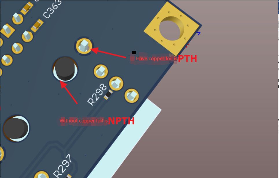
The difference of PTH NPTH in PCB through holes
It can be observed that there are many large and small holes in the circuit board, and it can be found that there are many dense holes, and each hole is designed for its purpose. These holes can basically be divided into PTH (Plating Through Hole) and NPTH (Non Plating Through Hole) plating throu...Read more -
PCB Silkscreen
PCB silk screen printing is an important process in the production of PCB circuit boards, which determines the quality of the finished PCB board. PCB circuit board design is very complicated. There are many small details in the design process. If it is not handled properly, it will affect the per...Read more -
Cause of PCB falling solder plate
PCB circuit board in the production process, often encounter some process defects, such as PCB circuit board copper wire off bad (is also often said to throw copper), affect product quality. The common reasons for PCB circuit board throwing copper are as follows: PCB circuit board process facto...Read more -
Flexible Printed Circuit
Flexible Printed Circuit Flexible Printed Circuit,It can be bent, wound and folded freely. The flexible circuit board is processed by using polyimide film as the base material. It is also called soft board or FPC in the industry. The process flow of flexible circuit board is divided into Double-...Read more -

Cause of PCB falling solder plate
Cause of PCB falling solder plate PCB circuit board in the production process, often encounter some process defects, such as PCB circuit board copper wire off bad (is also often said to throw copper), affect product quality. The common reasons for PCB circuit board throwing copper are as follows:...Read more -
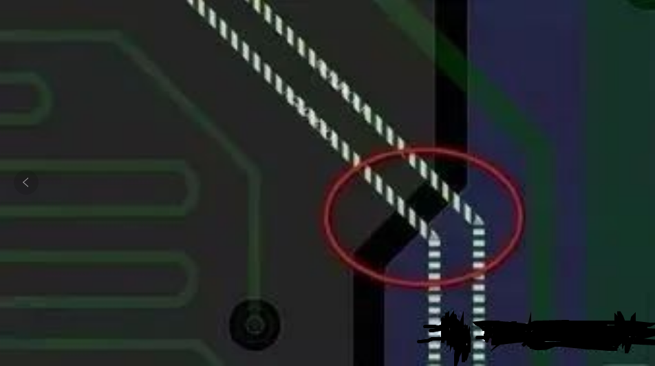
How to deal with PCB signal crossing divider line?
In the process of PCB design, the division of the power plane or the division of the ground plane will lead to the incomplete plane. In this way, when the signal is routed, its reference plane will span from one power plane to another power plane. This phenomenon is called signal span division. ...Read more -
Discussion on PCB electroplating hole filling process
The size of electronic products is becoming thinner and smaller, and directly stacking vias on blind vias is a design method for high-density interconnection. To do a good job of stacking holes, first of all, the flatness of the bottom of the hole should be done well. There are several manufactur...Read more -
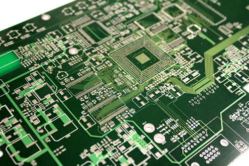
What is copper cladding?
1.Copper cladding The so-called copper coating, is the idle space on the circuit board as a datum, and then filled with solid copper, these copper areas are also known as copper filling. The significance of copper coating is: reduce ground impedance, improve anti-interference ability; Reduce volt...Read more -
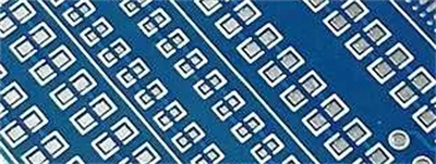
Types of PCB pads
1. Square pad It is often used when the components on the printed board are large and few, and the printed line is simple. When making a PCB by hand, using this pad is easy to achieve 2.Round pad Widely used in single-sided and double-sided printed boards, the parts are arranged regularl...Read more -
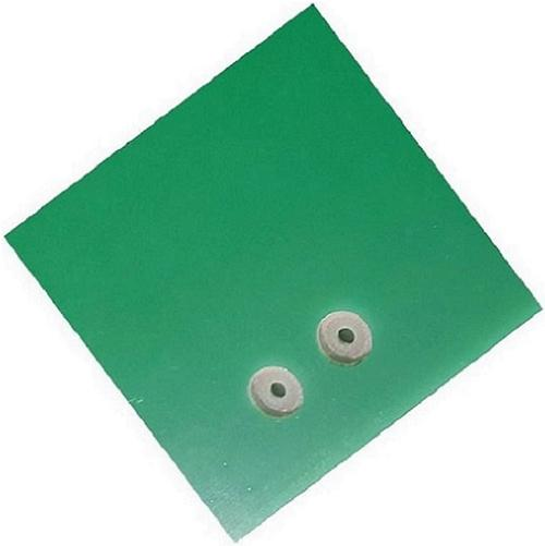
Counterbore
Countersunk holes are drilled on the circuit board with a flat head drill needle or gong knife, but cannot be drilled through (i.e., semi through holes). The transition part between the hole wall at the outermost/largest hole diameter and the hole wall at the smallest hole diameter is parallel to...Read more -
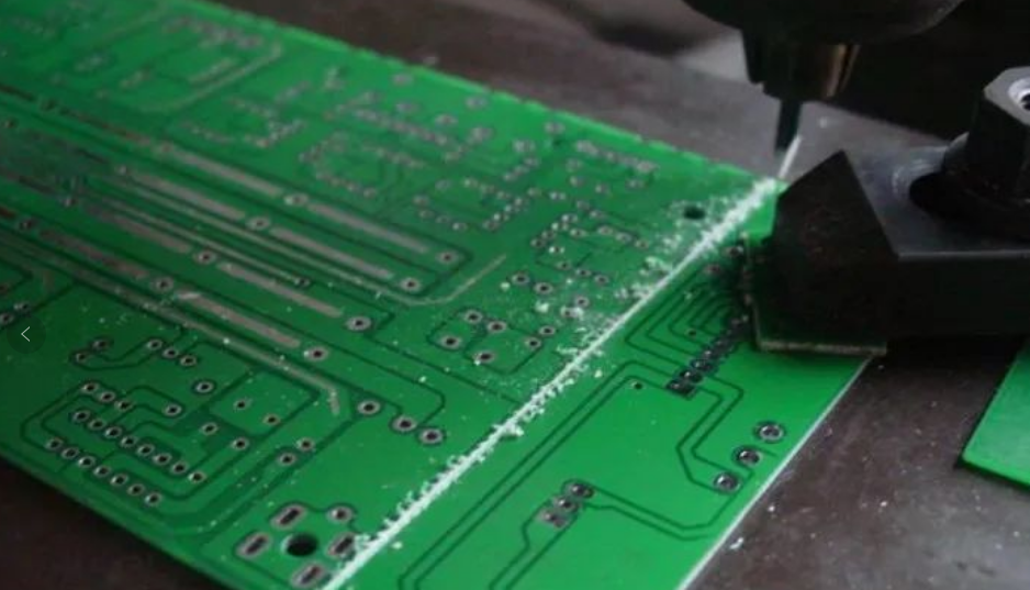
What is the role of the tooling strip with PCB?
In the PCB production process, there is another important process, that is, tooling strip. The reservation of process edge is of great significance for the subsequent SMT patch processing. The tooling strip is the part added on both sides or four sides of the PCB board, mainly to assist the SMT p...Read more -
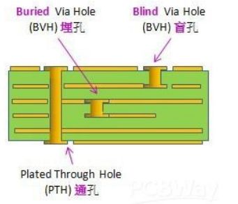
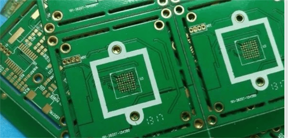
Introduction of Via-in-Pad:
Introduction of Via-in-Pad: It is well known that vias (VIA) can be divided into plated through hole, blind vias hole and buried vias hole, which have different functions. With the development of electronic products, vias play a vital role in the interlayer interconnection of printed circuit bo...Read more


