1.Design for Manufacturability of PCBA
The manufacturability design of PCBA mainly solves the problem of assemblability, and the purpose is to achieve the shortest process path, the highest soldering pass rate, and the lowest production cost. The design content mainly includes: process path design, component layout design on the assembly surface, pad and solder mask design (related to the pass-through rate), assembly thermal design, assembly reliability design, etc.
(1)PCBA Manufacturability
The manufacturability design of PCB focuses on “manufacturability”, and the design content includes plate selection, press-fit structure, annular ring design, solder mask design, surface treatment and panel design, etc. These designs are all related to the processing capability of the PCB. Limited by the processing method and capability, the minimum line width and line spacing, minimum hole diameter, minimum pad ring width, and minimum solder mask gap must conform to the PCB processing capability. The designed stack The layer and lamination structure must conform to the PCB processing technology. Therefore, the manufacturability design of PCB focuses on meeting the process capability of the PCB factory, and understanding the PCB manufacturing method, process flow and process capability is the basis for implementing process design.
(2)Assemblability of PCBA
The PCBA’s assembleability design focuses on “assemblability”, that is, to establish a stable and robust processability, and to achieve high-quality, high-efficiency and low-cost soldering. The content of the design includes package selection, pad design, assembly method (or process path design), component layout, steel mesh design, etc. All these design requirements are based on higher welding yield, higher manufacturing efficiency, and lower manufacturing cost.
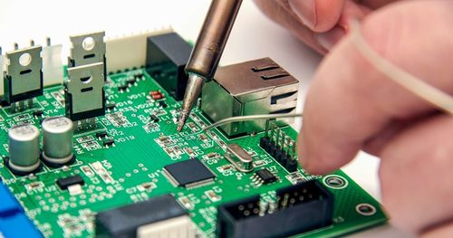
2.Laser soldering process
Laser soldering technology is to irradiate the pad area with a precisely focused laser beam spot. After absorbing the laser energy, the solder area heats up rapidly to melt the solder, and then stops the laser irradiation to cool the solder area and solidify the solder to form a solder joint. The welding area is locally heated, and other parts of the entire assembly are hardly affected by heat. The laser irradiation time during welding is usually only a few hundred milliseconds. Non-contact soldering, no mechanical stress on the pad, higher space utilization.
Laser welding is suitable for selective reflow soldering process or connectors using tin wire. If it is an SMD component, you need to apply solder paste first, and then solder. The soldering process is divided into two steps: first, the solder paste needs to be heated, and the solder joints are also preheated. After that, the solder paste used for soldering is completely melted, and the solder completely wets the pad, finally forming a solder joint. Using laser generator and optical focusing components for welding, high energy density, high heat transfer efficiency, non-contact welding, solder can be solder paste or tin wire, especially suitable for welding small solder joints in small spaces or small solder joints with low power, saving energy.
3.Laser welding design requirements for PCBA
(1) Automatic production PCBA transmission and positioning design
For automated production and assembly, the PCB must have symbols that conform to optical positioning, such as Mark points. Or the contrast of the pad is obvious, and the visual camera is positioned.
(2) The welding method determines the layout of components
Each welding method has its own requirements for the layout of components, and the layout of components must meet the requirements of the welding process. Scientific and reasonable layout can reduce bad solder joints and reduce the use of tooling.
(3) Design to improve welding pass-through rate
Matching design of pad, solder resist, and stencil The pad and pin structure determine the shape of the solder joint and also determine the ability to absorb molten solder. The rational design of the mounting hole achieves a tin penetration rate of 75%.