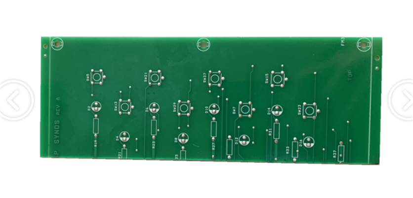
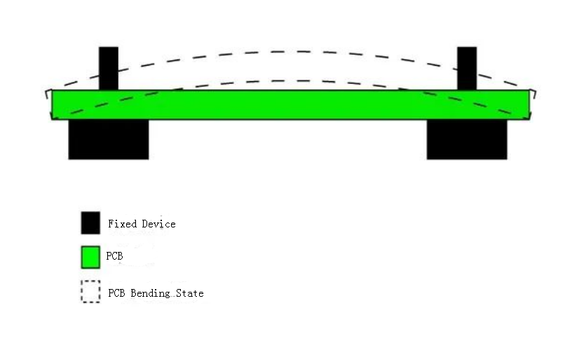
In fact, PCB warping also refers to the bending of the circuit board, which refers to the original flat circuit board. When placed on the desktop, the two ends or the middle of the board appear slightly upward. This phenomenon is known as PCB warping in the industry.
The formula for calculating the warpage of the circuit board is to lay the circuit board flat on the table with the four corners of the circuit board on the ground and measure the height of the arch in the middle. The formula is as follows:
Warpage = the height of the arch/the length of the PCB long side *100%.
Circuit board warpage industry standard: According to IPC — 6012(1996 edition) “Specification for Identification and Performance of Rigid Printed Boards”, the maximum warpage and distortion allowed for the production of circuit boards is between 0.75% and 1.5%. Due to the different process capabilities of each factory, there are also certain differences in PCB warpage control requirements. For 1.6 board thick conventional double-sided multilayer circuit boards, most circuit board manufacturers control the PCB warpage between 0.70-0.75%, many SMT, BGA boards, requirements within the range of 0.5%, some circuit board factories with strong process capacity can raise the PCB warpage standard to 0.3%.
How to avoid the warping of the circuit board during manufacturing?
(1)The semi-cured arrangement between each layer should be symmetrical, the proportion of six layers circuit boards, the thickness between 1-2 and 5-6 layers and the number of semi-cured pieces should be consistent;
(2)Multi-layer PCB core board and curing sheet should use the same supplier’s products;
(3)The outer A and B side of the line graphic area should be as close as possible, when the A side is a large copper surface, B side only a few lines, this situation is easy to occur after etching warping.
How to prevent circuit board warping?
1.Engineering design: interlayer semi-curing sheet arrangement should be appropriate; Multilayer core board and semi-cured sheet shall be made from the same supplier; The graphic area of the outer C/S plane is as close as possible, and an independent grid can be used.
2.Drying plate before blanking: generally 150 degrees 6-10 hours, exclude the water vapor in the plate, further make the resin curing completely, eliminate the stress in the plate; Baking sheet before opening, both inner layer and double side need!
3.Before laminates, attention should be paid to the warp and weft direction of solidified plate: the warp and weft shrinkage ratio is not the same, and attention should be paid to distinguish the warp and weft direction before laminating semi-solidified sheet; The core plate should also pay attention to the direction of warp and weft; The general direction of plate curing sheet is the meridian direction; The long direction of the copper clad plate is meridional; 10 layers of 4OZ power thick copper sheet
4.the thickness of the lamination to eliminate stress after cold pressing, trimming the raw edge;
5.Baking plate before drilling: 150 degrees for 4 hours;
6.It is better not to go through mechanical grinding brush, chemical cleaning is recommended; Special fixture is used to prevent the plate from bending and folding
7.After spraying tin on the flat marble or steel plate natural cooling to room temperature or air floating bed cooling after cleaning;