Compared with LDO, the circuit of DC-DC is much more complex and noisy, and the layout and layout requirements are higher. The quality of layout directly affects the performance of DC-DC, so it is very important to understand the layout of DC-DC
1. Bad layout
●EMI, DC-DC SW pin will have higher dv/dt, relatively high dv/dt will cause relatively large EMI interference;
●Ground noise, the ground line is not good, will produce relatively large switching noise on the ground wire, and these noises will affect other parts of the circuit;
●The voltage drop is generated on the wiring. If the wiring is too long, the voltage drop will be generated on the wiring, and the efficiency of the whole DC-DC will be reduced.
2. General principles
●Switch large current circuit as short as possible;
●The signal ground and the high-current ground (power ground) are routed separately and connected in a single point at the chip GND
①Short switching loop
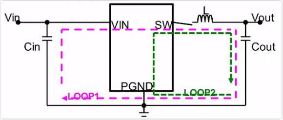
The red LOOP1 in the figure below is the current flow direction when the DC-DC high-side pipe is on and the low-side pipe is off. Green LOOP2 is the current flow direction when the high side pipe is closed and the low side pipe is opened;
In order to make the two loops as small as possible and introduce less interference, the following principles need to be followed:
●Inductance as close to SW pin as possible;
●Input capacitance as close to VIN pin as possible;
●The ground of the input and output capacitors should be close to the PGND pin.
●Use the way of laying copper wire;
Why would you do that?
●Too fine and too long a line will increase the impedance, and a large current will produce a relatively high ripple voltage in this large impedance;
●Too fine and too long a wire will increase the parasitic inductance, and the coupling switch noise on the inductance will affect the stability of DC-DC and cause EMI problems.
●The parasitic capacitance and impedance will increase the switching loss and on-off loss and affect the efficiency of DC-DC
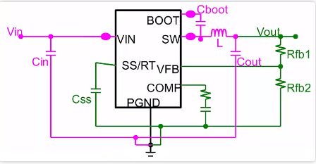
②single point grounding
Single point grounding refers to the single point grounding between signal ground and power ground. There will be relatively large switching noise on power ground, so it is necessary to avoid causing interference to sensitive small signals, such as FB feedback pin.
●High-current ground: L, Cin, Cout, Cboot connect to the network of high-current ground;
●Low current ground: Css, Rfb1, Rfb2 separately connected to the signal ground network;
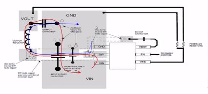
The following is the layout of a development board of TI. Red is the current path when the upper tube is opened, and blue is the current path when the lower tube is opened. The following layout has the following advantages:
●The GND of the input and output capacitors is connected with copper. When installing pieces, the ground of the two should be put together as far as possible.
●The current path of Dc-Dc-ton and Toff is very short;
●The small signal on the right is single-point grounding, which is far away from the influence of the large current switch noise on the left;
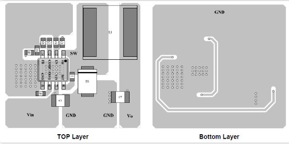
3. Examples
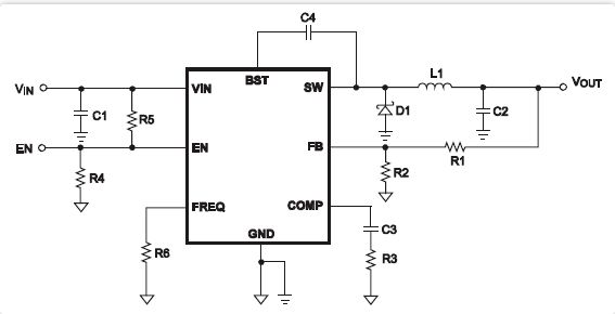
The layout of a typical DC-DC BUCK circuit is given below, and the following points are given in the SPEC:
●Input capacitors, high-edge MOS tubes, and diodes form switching loops that are as small and short as possible;
●Input capacitance as close as possible to Vin Pin pin;
●Ensure that all feedback connections are short and direct, and that feedback resistors and compensating elements are as close to the chip as possible;
●SW away from sensitive signals such as FB;
●Connect VIN, SW, and especially GND separately to a large copper area to cool the chip and improve thermal performance and long-term reliability;
4. Summarize
layout of DC-DC circuit is very important, which directly affects the working stability and performance of DC-DC. Generally, SPEC of DC-DC chip will give layout guidance, which can be referred to for design.