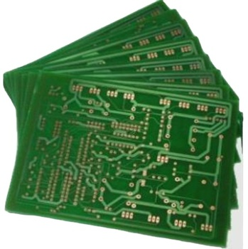
In the field of electronics, multi-layer PCB (Printed Circuit Board) plays a crucial role. Its design and manufacture have a profound impact on the performance and reliability of modern electronic equipment. This article will delve into its key features, design considerations, and application areas in order to provide a comprehensive perspective. By analyzing it, we can better understand its importance in electronic technology.
1, the design of multi-layer PCB board is not a simple stacking of multiple single-layer boards, but a complex engineering discipline. In the design phase, the first thing to consider is the complexity and density of the circuit. With the continuous pursuit of function in modern electronic devices, the complexity of circuits is also increasing, so its design needs to be able to meet the requirements of high density and multi-function. At the same time, the performance requirements of electronic devices are also increasing, and their design needs to ensure the stability and reliability of signal transmission.
2, the manufacturing process of multi-layer PCB board is also a key part. In the manufacturing phase, advanced processes and technologies are crucial. By using advanced lamination technology, the quality of interlayer connection can be effectively improved to ensure the stability of signal transmission. In addition, the appropriate material selection is also a factor that can not be ignored in the manufacturing process, different application fields have different requirements for materials, so it is necessary to choose the appropriate material according to the specific application scenario in manufacturing.
3, multi-layer PCB board has a wide range of applications in the field of electronics. First of all, it plays a core role in high-end electronic equipment, such as communication equipment, computer hardware and so on. Its high density and stability allow these devices to better meet the performance requirements of users. Secondly, in the field of automotive electronics, it is also widely used in vehicle electronic systems, such as navigation, entertainment and so on. Due to the high reliability and durability requirements of automotive electronics, multi-layer PCB boards have become an indispensable component. In addition, it has also shown its unique advantages in the fields of medical equipment, industrial control and so on.
First, let’s focus on the manufacturing process of PCB double-layer boards. Modern PCB manufacturing often uses advanced chemical etching techniques to form circuit patterns by covering the pattern on a copper overlay and then using a chemical solution to corrode the unwanted parts. This process requires not only high-precision equipment, but also strict process control to ensure the quality and stability of the board. In the continuous development of PCB manufacturing, new processes and materials continue to emerge, providing strong support for its performance improvement.
In the field of application, PCB double-layer board has been widely used in all kinds of electronic equipment. From consumer electronics to industrial controls, from medical devices to communication systems, it plays a vital role. Its stable electrical performance and good reliability make it an indispensable part of modern electronic products. At the same time, its design flexibility also provides more possibilities for various applications, to meet the specific needs of different fields for the board.
However, with the continuous innovation and diversification of electronic products, the requirements for PCB double-layer boards are also increasing. In the future, we can look forward to the possibility of higher density and higher rate PCB double-layer boards to meet the needs of a new generation of electronic devices. The continuous breakthrough of advanced material technology and manufacturing process will promote its development in the direction of thinner and higher performance, opening up new space for innovation in electronic products.
1. Let’s have an in-depth understanding of the specific structure of the 4-layer PCB board.
A board usually consists of two layers of an inner conductor and two layers of an outer substrate. The inner conductor layer is responsible for connecting various electronic components to form the circuit, while the outer substrate layer acts as a support and insulation. This design allows electronic engineers to arrange circuit components more flexibly, improving the integration and performance of the circuit.
2, the structural advantage of 4-layer PCB board is its good signal isolation performance.
The inner conductor layer is separated by electrical insulation material, effectively isolating the different levels of signal. This signal isolation performance is critical for complex electronic devices, especially in high frequency and high density applications.Through reasonable design and layout of the internal layer, the 4-layer PCB board can reduce signal interference, improve circuit stability, and ensure the reliability of the equipment.
3, 4 layer PCB board structure design is also conducive to heat dissipation.
Electronic devices generate a lot of heat during operation, and effective heat dissipation is essential to maintain the normal operation of the equipment. The 4-layer PCB board also increases the thermal conductivity channel by increasing the internal conductor layer, which helps to transfer and dissipate heat. This allows the electronic equipment to better maintain a stable temperature during high load operation, extending the service life of the equipment.
4, 4-layer PCB board also performs well in terms of wiring.
The inner conductor layer allows for a more complex and compact wiring design, reducing the space footprint of the circuit. This is essential for lightweight and miniaturized electronic device design. At the same time, the complex wiring design also provides the possibility for the integration of different functional modules, so that the electronic device can maintain strong functional performance while being small.
The 4-layer PCB board structure plays an important role in modern electronic engineering, and its unique structural design provides flexibility, performance stability and heat dissipation for electronic devices, making it ideal for a variety of applications. With the continuous development of science and technology, we can expect 4-layer PCB boards to show a wider range of applications in more fields, bringing more innovation and breakthroughs to electronic engineering.
Taken together, multi-layer PCB board as a key component in modern electronic technology, its design and manufacturing is crucial. In the circuit design stage, the complexity and density of the circuit should be considered. In the manufacturing stage, it is necessary to use advanced processes and technologies and choose the right materials. Its wide range of applications covers many fields such as communications, computers, and automobiles, providing a solid foundation for the performance and reliability of various electronic devices. In the future, with the continuous development of electronic technology, its design and manufacturing will continue to face new challenges, but it will also provide a broader space for the development of electronic devices.