According to the product structure, it can be divided into rigid board (hard board), flexible board (soft board), rigid flexible joint board, HDI board and package substrate. According to the number of line layer classification, PCB can be divided into single panel, double panel and multi-layer board.
Rigid plate
Product characteristics: It is made of rigid substrate which is not easy to bend and has certain strength. It has bending resistance and can provide certain support for electronic components attached to it. The rigid substrate includes glass fiber cloth substrate, paper substrate, composite substrate, ceramic substrate, metal substrate, thermoplastic substrate, etc.
Applications: Computer and network equipment, communication equipment, industrial control and medical, consumer electronics and automotive electronics.
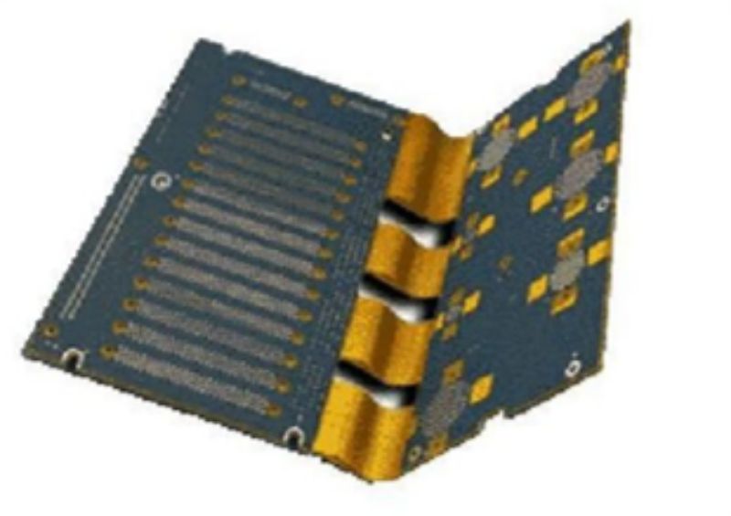
Flexible plate
Product characteristics: It refers to the printed circuit board made of flexible insulating substrate. It can be freely bent, wound, folded, arbitrarily arranged according to the spatial layout requirements, and arbitrarily moved and expanded in three-dimensional space. Thus, component assembly and wire connection can be integrated.
Applications: smart phones, laptops, tablets and other portable electronic devices.
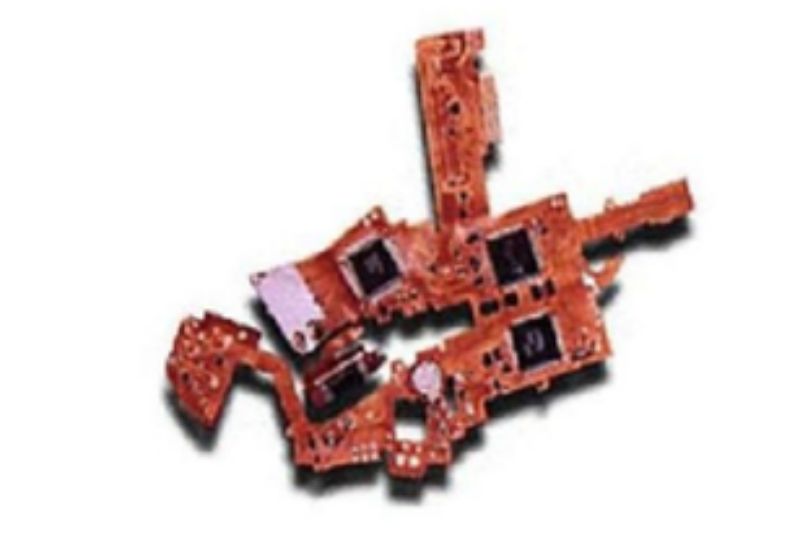
Rigid torsion bonding plate
Product characteristics: refers to a printed circuit board containing one or more rigid areas and flexible areas, the thin layer of flexible printed circuit board bottom and rigid printed circuit board bottom combined lamination. Its advantage is that it can provide the support role of rigid plate, but also has the bending characteristics of flexible plate, and can meet the needs of three-dimensional assembly.
Applications: Advanced medical electronic equipment, portable cameras and folding computer equipment.
HDI board
Product features: High Density Interconnect abbreviation, that is, high density interconnect technology, is a printed circuit board technology. HDI board is generally manufactured by layering method, and laser drilling technology is used to drill holes in the layering, so that the whole printed circuit board forms interlayer connections with buried and blind holes as the main conduction mode. Compared with the traditional multi-layer printed board, HDI board can improve the wiring density of the board, which is conducive to the use of advanced packaging technology. The signal output quality can be improved; It can also make electronic products more compact and convenient in appearance.
Application: Mainly in the field of consumer electronics with high density demand, it is widely used in mobile phones, notebook computers, automotive electronics and other digital products, among which mobile phones are the most widely used. At present, communication products, network products, server products, automotive products and even aerospace products are used in HDI technology.
Package substrate
Product features: that is, IC seal loading plate, which is directly used to carry the chip, can provide electrical connection, protection, support, heat dissipation, assembly and other functions for the chip, in order to achieve multi-pin, reduce the size of the package product, improve the electrical performance and heat dissipation, ultra-high density or the purpose of multi-chip modularization.
Application field: In the field of mobile communication products such as smart phones and tablet computers, packaging substrates have been widely used. Such as memory chips for storage, MEMS for sensing, RF modules for RF identification, processor chips and other devices should use packaging substrates. The high speed communication package substrate has been widely used in data broadband and other fields.
The second type is classified according to the number of line layers. According to the number of line layer classification, PCB can be divided into single panel, double panel and multi-layer board.
Single panel
Single-Sided Boards (single-sided Boards) On the most basic PCB, the parts are concentrated on one side, the wire is concentrated on the other side (there is a patch component and the wire is the same side, and the plug-in device is the other side). Because the wire only appears on one side, this PCB is called Single-sided. Because a single panel has many strict restrictions on the design circuit (because there is only one side, the wiring can not cross and must go around a separate path), only early circuits used such boards.
Dual panel
Double-Sided Boards have wiring on both sides, but to use wires on both sides, there must be a proper circuit connection between the two sides. This “bridge” between circuits is called a pilot hole (via). A pilot hole is a small hole filled with or coated with metal on the PCB, which can be connected with wires on both sides. Because the area of the double panel is twice as large as that of the single panel, the double panel solves the difficulty of the wiring interleaving in the single panel (it can be channeled through the hole to the other side), and it is more suitable for use in more complex circuits than the single panel.
Multi-Layer Boards In order to increase the area that can be wired, multi-layer boards use more single or double sided wiring boards.
A printed circuit board with a double-sided inner layer, two single-sided outer layer or two double-sided inner layer, two single-sided outer layer, through the positioning system and insulating binder materials alternately together and the conductive graphics are interconnected according to the design requirements of the printed circuit board becomes a four-layer, six-layer printed circuit board, also known as multi-layer printed circuit board.
The number of layers of the board does not mean that there are several independent wiring layers, and in special cases, empty layers will be added to control the thickness of the board, usually the number of layers is even, and contains the outermost two layers. Most of the host board is a 4 to 8 layer structure, but technically it is possible to achieve nearly 100 layers of PCB board. Most large supercomputers use a fairly multilayer mainframe, but since such computers can be replaced by clusters of many ordinary computers, ultra-multilayer boards have fallen out of use. Because the layers in the PCB are closely combined, it is generally not easy to see the actual number, but if you carefully observe the host board, it can still be seen.