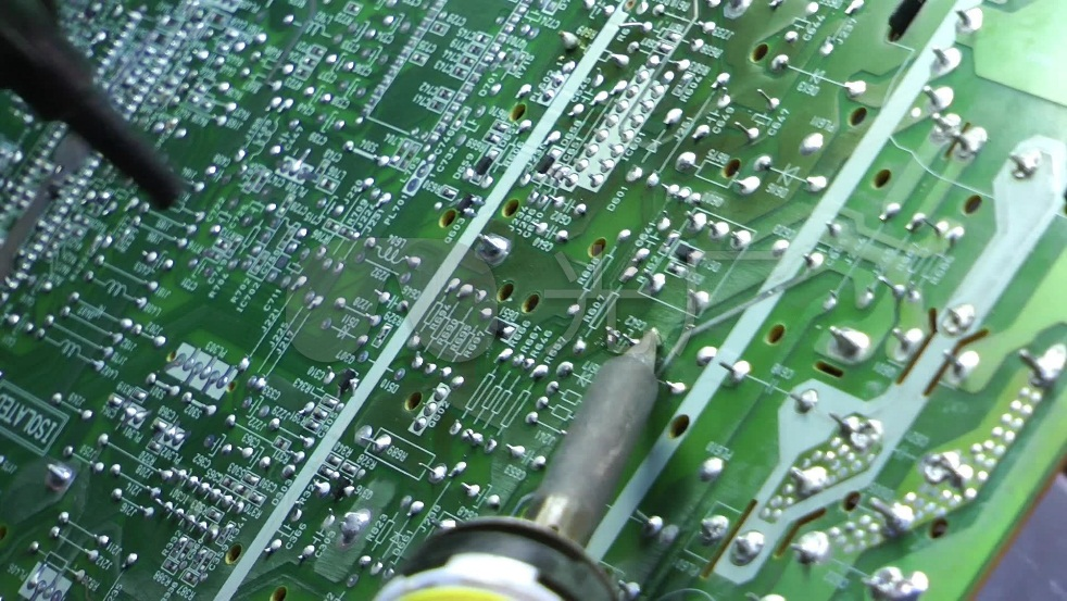
In PCBA processing, the welding quality of the circuit board has a great impact on the performance and appearance of the circuit board. Therefore, it is very important to control the welding quality of the PCB circuit board. PCB circuit board welding quality is closely related to circuit board design, process materials, welding technology and other factors.
一、Design of PCB circuit board
1. Pad design
(1) When designing the pads of plug-in components, the pad size should be designed appropriately. If the pad is too large, the solder spreading area is large, and the solder joints formed are not full. On the other hand, the surface tension of the copper foil of the smaller pad is too small, and the solder joints formed are non-wetting solder joints. The matching gap between the aperture and component leads is too large and it is easy to cause false soldering. When the aperture is 0.05 – 0.2mm wider than the lead and the pad diameter is 2 – 2.5 times the aperture, it is an ideal condition for welding.
(2) When designing the pads of chip components, the following points should be considered: In order to eliminate the “shadow effect” as much as possible, the soldering terminals or pins of the SMD should face the direction of the tin flow to facilitate contact with the tin flow. Reduce false soldering and missing soldering. Smaller components should not be placed after larger components to prevent the larger components from interfering with the solder flow and contacting the pads of the smaller components, resulting in soldering leaks.
2、 PCB circuit board flatness control
Wave soldering has high requirements on the flatness of printed boards. Generally, the warpage is required to be less than 0.5mm. If it is greater than 0.5mm, it needs to be flattened. In particular, the thickness of some printed boards is only about 1.5mm, and their warpage requirements are higher. Otherwise, the welding quality cannot be guaranteed. The following matters should be paid attention to:
(1) Properly store printed boards and components and shorten the storage period as much as possible. During welding, copper foil and component leads free of dust, grease, and oxides are conducive to the formation of qualified solder joints. Therefore, printed boards and components should be stored in a dry place. , in a clean environment, and shorten the storage period as much as possible.
(2) For printed boards that have been placed for a long time, the surface generally needs to be cleaned. This can improve the solderability and reduce false soldering and bridging. For component pins with a certain degree of surface oxidation, the surface should be removed first. oxide layer.
二. Quality control of process materials
In wave soldering, the main process materials used are: flux and solder.
1. The application of flux can remove oxides from the welding surface, prevent re-oxidation of the solder and the welding surface during welding, reduce the surface tension of the solder, and help transfer heat to the welding area. Flux plays an important role in the control of welding quality.
2. Quality control of solder
Tin-lead solder continues to oxidize at high temperatures (250°C), causing the tin content of the tin-lead solder in the tin pot to continuously decrease and deviate from the eutectic point, resulting in poor fluidity and quality problems such as continuous soldering, empty soldering, and insufficient solder joint strength. .
三、Welding process parameter control
The influence of welding process parameters on welding surface quality is relatively complex.
There are several main points: 1. Control of preheating temperature. 2. Welding track inclination angle. 3. Wave crest height. 4. Welding temperature.
Welding is an important process step in the PCB circuit board production process. In order to ensure the welding quality of the circuit board, one should be proficient in quality control methods and welding skills.
