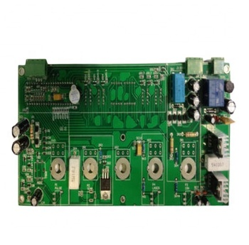
The PCBA production process can be divided into several major processes:
PCB design and development →SMT patch processing →DIP plug-in processing →PCBA test → three anti-coating → finished product assembly.
First, PCB design and development
1.Product demand
A certain scheme can obtain a certain profit value in the current market, or enthusiasts want to complete their own DIY design, then the corresponding product demand will be generated;
2. Design and development
Combined with the customer’s product needs, R & D engineers will choose the corresponding chip and external circuit combination of PCB solution to achieve product needs, this process is relatively long, the content involved here will be described separately;
3, sample trial production
After the development and design of the preliminary PCB, the purchaser will purchase the corresponding materials according to the BOM provided by the research and development to carry out the production and debugging of the product, and the trial production is divided into proofing (10pcs), secondary proofing (10pcs), small batch trial production (50pcs~100pcs), large batch trial production (100pcs~3001pcs), and then will enter the mass production stage.
Second, SMT patch processing
The sequence of SMT patch processing is divided into: material baking → solder paste access →SPI→ mounting → reflow soldering →AOI→ repair
1. Materials baking
For chips, PCB boards, modules and special materials that have been in stock for more than 3 months, they should be baked at 120℃ 24H. For MIC microphones, LED lights and other objects that are not resistant to high temperature, they should be baked at 60℃ 24H.
2, solder paste access (return temperature → stirring → use)
Because our solder paste is stored in the environment of 2~10℃ for a long time, it needs to be returned to the temperature treatment before use, and after the return temperature, it needs to be stirred with a blender, and then it can be printed.
3. SPI3D detection
After the solder paste is printed on the circuit board, the PCB will reach the SPI device through the conveyor belt, and the SPI will detect the thickness, width, length of the solder paste printing and the good condition of the tin surface.
4. Mount
After the PCB flows to the SMT machine, the machine will select the appropriate material and paste it to the corresponding bit number through the set program;
5. Reflow welding
The pcb filled with material flows to the front of reflow welding, and passes through ten step temperature zones from 148℃ to 252℃ in turn, safely bonding our components and PCB board together;
6, online AOI testing
AOI is an automatic optical detector, which can check the PCB board just out of the furnace through high-definition scanning, and can check whether there is less material on the PCB board, whether the material is shifted, whether the solder joint is connected between the components and whether the tablet is offset.
7. Repair
For the problems found on the PCB board in AOI or manually, it needs to be repaired by the maintenance engineer, and the repaired PCB board will be sent to the DIP plug-in together with the normal offline board.
Three, DIP plug-in
The process of DIP plug-in is divided into: shaping → plug-in → wave soldering → cutting foot → holding tin → washing plate → quality inspection
1. Plastic Surgery
The plug-in materials we bought are all standard materials, and the pin length of the materials we need is different, so we need to shape the feet of the materials in advance, so that the length and shape of the feet are convenient for us to carry out plug-in or post welding.
2. Plug-in
The finished components will be inserted according to the corresponding template;
3, wave soldering
The inserted plate is placed on the jig to the front of the wave soldering. First, the flux will be sprayed at the bottom to help welding. When the plate comes to the top of the tin furnace, the tin water in the furnace will float and contact the pin.
4. Cut the feet
Because the pre-processing materials will have some specific requirements to set aside a slightly longer pin, or the incoming material itself is not convenient to process, the pin will be trimmed to the appropriate height by manual trimming;
5. Holding tin
There may be some bad phenomena such as holes, pinholes, missed welding, false welding and so on in the pins of our PCB board after furnace. Our tin holder will repair them by manual repair.
6. Wash the board
After the wave soldering, repair and other front-end links, there will be some residual flux or other stolen goods attached to the pin position of the PCB board, which requires our staff to clean its surface;
7. Quality inspection
PCB board components error and leakage check, unqualified PCB board needs to be repaired, until qualified to proceed to the next step;
4. PCBA test
PCBA test can be divided into ICT test, FCT test, aging test, vibration test, etc
PCBA test is a big test, according to different products, different customer requirements, the test means used are different. ICT test is to detect the welding condition of components and the on-off condition of lines, while FCT test is to detect the input and output parameters of PCBA board to check whether they meet the requirements.
Five: PCBA three anti-coating
PCBA three anti-coating process steps are: brushing side A → surface dry → brushing side B → room temperature curing 5. Spraying thickness:
0.1mm-0.3mm6. All coating operations shall be carried out at a temperature not lower than 16℃ and relative humidity below 75%. PCBA three anti-coating is still a lot of, especially some temperature and humidity more harsh environment, PCBA coating three anti-paint has superior insulation, moisture, leakage, shock, dust, corrosion, anti-aging, anti-mildew, anti-parts loose and insulation corona resistance performance, can extend the storage time of PCBA, isolation of external erosion, pollution and so on. Spraying method is the most commonly used coating method in the industry.
Finished product assembly
7.The coated PCBA board with the test OK is assembled for the shell, and then the whole machine is aging and testing, and the products without problems through the aging test can be shipped.
PCBA production is a link to a link. Any problem in the pcba production process will have a great impact on the overall quality, and each process needs to be strictly controlled.