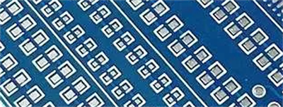
1. Square pad
It is often used when the components on the printed board are large and few, and the printed line is simple. When making a PCB by hand, using this pad is easy to achieve
2.Round pad
Widely used in single-sided and double-sided printed boards, the parts are arranged regularly. If the density of the board allows, the pads can be larger and will not fall off during soldering.
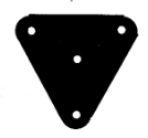
3. Island shape pad
The pad-to-pad connections are integrated. Commonly used in vertical irregular arrangement installation。
4. Polygon Pad
It is used to distinguish gaskets with similar outer diameters and different hole diameters, which is convenient for processing and assembly
5. Oval PadThe pad has enough area to enhance the anti-stripping ability, often used in dual in-line devices
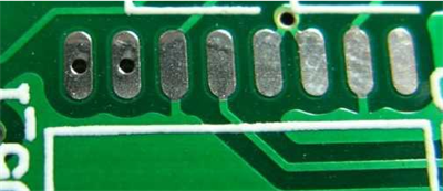
6.Open-shaped Pad
In order to ensure that after wave soldering, the pad holes for manual soldering will not be blocked by solder.
7. cross pad
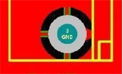
Cross-shaped pads are also called thermal pads, hot air pads, etc. Its function is to reduce the heat dissipation of the welding plate during welding, and prevent false welding or PCB peeling caused by excessive heat dissipation.
● When your pads are ground. The cross-shaped flower can reduce the connection area of the ground wire, slow down the heat dissipation speed, and facilitate welding.
● When your PCB needs machine placement and needs a reflow soldering machine, the cross-shaped pad can prevent the PCB from peeling off (because more heat is needed to melt the solder paste)
8. teardrop pad
It is typically used when the trace attached to the liner is thin, to prevent peeling of the liner and disconnection of the trace from the liner. This liner is often used in high frequency circuits