News
-
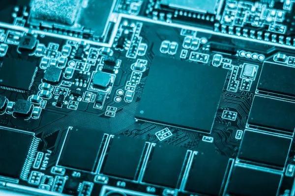
How to quickly determine the number of layers, wiring and layout of the PCB?
As PCB size requirements become smaller and smaller, device density requirements become higher and higher, and PCB design becomes more difficult. How to achieve a high PCB layout rate and shorten the design time, then we will talk about the design skills of PCB planning, layout and wiring.Read more -
The difference and function of circuit board soldering layer and solder mask
Introduction to Solder Mask The resistance pad is soldermask, which refers to the part of the circuit board to be painted with green oil. In fact, this solder mask uses a negative output, so after the shape of the solder mask is mapped to the board, the solder mask is not painted with green oil, ...Read more -
PCB plating has several methods
There are four main electroplating methods in circuit boards: finger-row electroplating, through-hole electroplating, reel-linked selective plating, and brush plating. Here is a brief introduction: 01 Finger row plating Rare metals need to be plated on the board edge connectors, board ed...Read more -
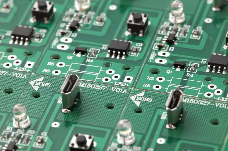
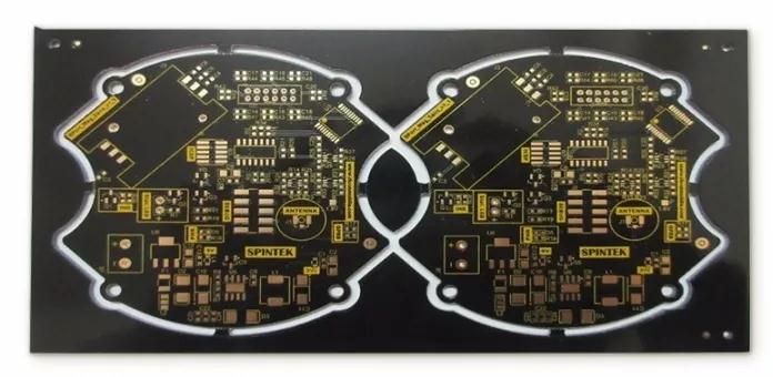
Quickly learn irregular-shaped PCB design
The complete PCB we envision is usually a regular rectangular shape. Although most designs are indeed rectangular, many designs require irregularly shaped circuit boards, and such shapes are often not easy to design. This article describes how to design irregular-shaped PCBs. Nowadays, the size o...Read more -
Through hole, blind hole, buried hole, what are the characteristics of the three PCB drilling?
Via (VIA), this is a common hole used to conduct or connect copper foil lines between conductive patterns in different layers of the circuit board. For example (such as blind holes, buried holes), but can not insert component leads or copper-plated holes of other reinforced materials. Because the...Read more -
How to make the most cost-effective PCB project? !
As a hardware designer, the job is to develop PCBs on time and within budget, and they need to be able to work normally! In this article, I will explain how to consider the manufacturing issues of the circuit board in the design, so that the cost of the circuit board is lower without affecting th...Read more -
PCB manufacturers have laid out Mini LED industry chain
Apple is about to launch Mini LED backlight products, and TV brand manufacturers have also successively introduced Mini LED. Previously, some manufacturers have launched Mini LED notebooks, and related business opportunities have gradually emerged. The legal person expects that PCB factories such...Read more -
Knowing this, do you dare to use expired PCB?
This article mainly introduces three hazards of using expired PCB. 01 Expired PCB may cause surface pad oxidation Oxidation of the soldering pads will cause poor soldering, which may eventually lead to functional failure or risk of dropouts. Different surface treatments of circuit boards w...Read more -
Why does PCB dump copper?
A. PCB factory process factors 1. Excessive etching of copper foil The electrolytic copper foil used in the market is generally single-sided galvanized (commonly known as ashing foil) and single-sided copper plating (commonly known as red foil). The common copper foil is generally galvanized copp...Read more -
How to reduce PCB design risks?
During the PCB design process, if possible risks can be predicted in advance and avoided in advance, the success rate of PCB design will be greatly improved. Many companies will have an indicator of the success rate of PCB design one board when evaluating projects. The key to improving the succe...Read more -
SMT skills 丨 component placement rules
In PCB design, the layout of components is one of the important links. For many PCB engineers, how to lay out components reasonably and effectively has its own set of standards. We summed up the layout skills, roughly the following 10 The layout of electronic components needs to be follow...Read more -
What role do those “special pads” on the PCB play?
1. Plum blossom pad. 1: The fixing hole needs to be non-metallized. During wave soldering, if the fixing hole is a metalized hole, tin will block the hole during reflow soldering. 2. Fixing mounting holes as quincunx pads is generally used for mounting hole GND network, because generally...Read more


