News
-
PCB Terms
Annular ring – a copper ring on a metalized hole on a PCB. DRC – Design rule check. A procedure to check whether the design contains errors, such as short circuits, too thin traces, or too small holes. Drilling hit – used to indicate the deviation between the drilling positi...Read more -
In PCB design, why is the difference between analog circuit and digital circuit so big?
The number of digital designers and digital circuit board design experts in the engineering field is constantly increasing, which reflects the development trend of the industry. Although the emphasis on digital design has brought about major developments in electronic products, it still exists, a...Read more -
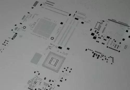
How to make high PCB precision?
The high-precision circuit board refers to the use of fine line width/spacing, micro holes, narrow ring width (or no ring width) and buried and blind holes to achieve high density. High precision means that the result of “fine, small, narrow, and thin” will inevitably lead to high pre...Read more -
A must for masters, so PCB production is simple and efficient!
Panelization is a way to maximize the profits of the circuit board manufacturing industry. There are many ways to panelize and non-panel circuit boards, as well as some challenges in the process. Producing printed circuit boards can be an expensive process. If the operation is not correct, the ci...Read more -

Challenges of 5G technology to high-speed PCB
What does this mean for the high-speed PCB industry? First of all, when designing and constructing PCB stacks, material aspects must be prioritized. 5G PCBs must meet all specifications when carrying and receiving signal transmission, providing electrical connections, and providing control for s...Read more -
5 tips can help you reduce PCB manufacturing costs.
01 Minimize the board size One of the main factors that can have a significant impact on production costs is the size of the printed circuit board. If you need a larger circuit board, the wiring will be easier, but the production cost will also be higher. vice versa. If your PCB is too small, a...Read more -
Disassemble iPhone 12 and iPhone 12 Pro to see whose PCB is inside
The iPhone 12 and iPhone 12 Pro were just launched, and the well-known dismantling agency iFixit immediately conducted a dismantling analysis of the iPhone 12 and iPhone 12 Pro. Judging from the dismantling results of iFixit, the new machine’s workmanship and materials are still excellent, ...Read more -
Basic rules of component layout
1. Layout according to circuit modules, and related circuits that realize the same function are called a module. The components in the circuit module should adopt the principle of nearby concentration, and the digital circuit and the analog circuit should be separated; 2. No components or devices...Read more -
How to use copper weight to make high-end PCB manufacturing ?
For many reasons, there are many different types of PCB manufacturing projects that require specific copper weights. We receive questions from customers who are not familiar with the concept of copper weight from time to time, so this article aims to solve these problems. In addition, the followi...Read more -

Pay attention to these things about PCB “layers”!
The design of a multilayer PCB (printed circuit board) can be very complicated. The fact that the design even requires the use of more than two layers means that the required number of circuits will not be able to be installed only on the top and bottom surfaces. Even when the circuit does fit in...Read more -
Specification terms for materials of 12-layer PCB
Several material options can be used to customize 12-layer PCB boards. These include different kinds of conductive materials, adhesives, coating materials, and so on. When specifying material specifications for 12-layer PCBs, you may find that your manufacturer uses many technical terms. You must...Read more -
PCB stackup design method
The laminated design mainly complies with two rules: 1. Each wiring layer must have an adjacent reference layer (power or ground layer); 2. The adjacent main power layer and ground layer should be kept at a minimum distance to provide larger coupling capacitance; The following lists the st...Read more


