1.Copper cladding
The so-called copper coating, is the idle space on the circuit board as a datum, and then filled with solid copper, these copper areas are also known as copper filling.
The significance of copper coating is: reduce ground impedance, improve anti-interference ability; Reduce voltage drop, improve power efficiency; Connected with the ground wire, it can also reduce the area of the loop.
Also for the purpose of making PCB welding as deformation as possible, most PCB manufacturers will also require PCB designers to fill the open area of PCB with copper or grid ground wire. If the copper is not properly handled, it will be more than worth the loss. Whether the copper is “more good than bad” or “more bad than good”? As we all know, in the case of high frequency, the distributed capacitance of the wiring on the printed circuit board will work. When the length is greater than 1/20 of the wavelength corresponding to the noise frequency, the antenna effect will be generated, and the noise will be emitted outwards through the wiring. If there is a poorly grounded copper coating in the PCB, the copper coating will become a tool to propagate the noise.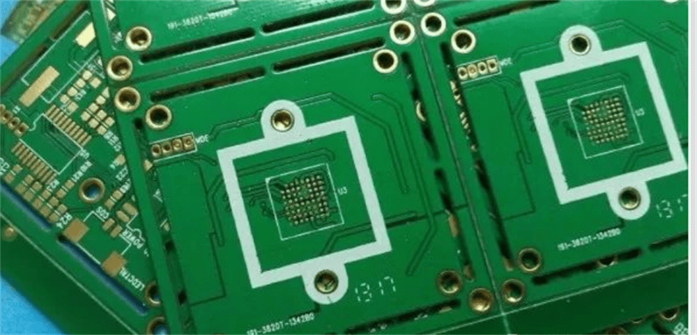
Therefore, in the high frequency circuit, do not think that the ground somewhere, this is the “ground wire”, must be less than λ/20 spacing, in the wiring through the hole, and the ground plane of the multilayer “good grounding”. If the copper coating is properly treated, the copper coating not only increases the current, but also plays the dual role of shielding interference. Therefore, in the high frequency circuit, do not think that the ground somewhere, this is the “ground wire”, must be less than λ/20 spacing, in the wiring through the hole, and the ground plane of the multilayer “good grounding”. If the copper coating is properly treated, the copper coating not only increases the current, but also plays the dual role of shielding interference.
2.Two forms of copper coating
There are generally two basic ways to cover copper, that is, large area of copper and grid copper, it is often asked that large area of copper or grid copper is good, not good to generalize.
Why? Large area of copper coating, with increasing the current and shielding dual role, but large area of copper coating, if the wave soldering, the board may tilt up, or even bubble. Therefore, a large area of copper is covered, and several slots are generally opened to alleviate copper foil foaming.
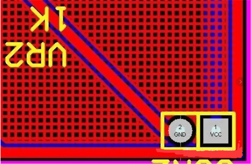
The simple grid covered with copper is mainly shielding effect, the role of increasing the current is reduced, from the point of view of heat dissipation, grid has advantages (it reduces the heating surface of copper) and plays a certain role of electromagnetic shielding. Especially for the touch circuit, as shown in the figure below: It is necessary to point out that the grid is composed of staggered lines. We know that for the circuit, the width of the lines has its corresponding “electrical length” to the working frequency of the circuit board (the actual size can be divided by the digital frequency corresponding to the working frequency, see relevant books for details).
When the operating frequency is not very high, maybe the grid lines are not very useful, and once the electrical length matches the operating frequency, it’s very bad, and you find that the circuit is not working properly at all, and there are signals everywhere that interfere with the system.
The suggestion is to choose according to the design of the circuit board, not to hold on to a thing. Therefore, high frequency circuit against interference requirements of the multi-purpose grid, low frequency circuit with large current circuit and other commonly used complete copper paving.