PCB silk screen printing is an important process in the production of PCB circuit boards, which determines the quality of the finished PCB board. PCB circuit board design is very complicated. There are many small details in the design process. If it is not handled properly, it will affect the performance of the entire PCB board. In order to maximize design efficiency and product quality, what issues should we pay attention to during design?
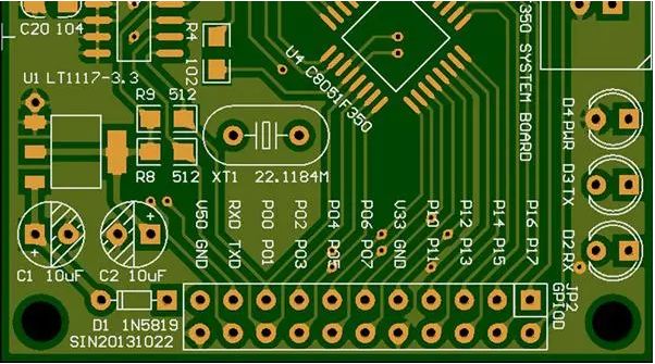
The character graphics are formed on the pcb board by silk screen or inkjet printing. Each character represents a different component and plays a very important role in the later design.
Let me introduce the common characters. Generally, C stands for capacitor, R stands for resistor, L stands for inductor, Q stands for transistor, D stands for diode, Y stands for crystal oscillator, U stands for integrated circuit, B stands for buzzer, T stands for transformer, K stands for Relays and more。
On the circuit board, we often see numbers such as R101, C203, etc. In fact, the first letter represents the component category, the second number identifies the circuit function number, and the third and fourth digits represent the serial number on the circuit board. So we understand very well that R101 is the first resistor on the first functional circuit, and C203 is the third capacitor on the second functional circuit, so that the character identification is easy to understand.
In fact, the characters on the PCB circuit board are what we often call the silk screen. The first thing consumers see when they get a PCB board is the silk screen on it. Through the silk screen characters, they can clearly understand what components should be placed in each position during installation. Easy to assemble patch and repair. So what problems should be paid attention to in the design process of silk screen printing?
1) The distance between the silk screen and the pad: the silk screen cannot be placed on the pad. If the pad is covered by the silk screen, it will affect the soldering of components, so a 6-8mil spacing should be reserved.2) Screen printing width: The screen printing line width is generally more than 0.1mm (4 mill), which refers to the width of the ink. If the line width is too small, the ink will not come out of the screen printing screen, and characters cannot be printed.3) Character height of silk screen printing: The character height is generally above 0.6mm (25mil). If the character height is less than 25mil, the printed characters will be unclear and easily blurred. If the character line is too thick or the distance is too close, it will cause blur.
4) The direction of silk screen printing: generally follow the principle of from left to right and from bottom to top.
5) Polarity definition: Components generally have polarity. The screen printing design should pay attention to marking the positive and negative poles and directional components. If the positive and negative poles are reversed, it is easy to cause a short circuit, causing the circuit board to burn and cannot be covered .
6) Pin identification: The pin identification can distinguish the direction of the components. If the silk screen characters mark the identification wrongly or there is no identification, it is easy to cause the components to be mounted in reverse.
7) Silk screen position: Do not place the silk screen design on the drilled hole, otherwise the printed pcb board will have incomplete characters.
There are many specifications and requirements for PCB silk screen design, and it is these specifications that promote the development of PCB screen printing technology.