1. The formation of slots during the PCB design process includes:
Slotting caused by the division of power or ground planes; when there are many different power supplies or grounds on the PCB, it is generally impossible to allocate a complete plane for each power supply network and ground network. The common approach is to Or perform power division or ground division on multiple planes. Slots are formed between different divisions on the same plane.
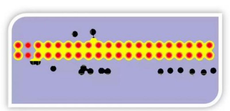
The through holes are too dense to form slots (through holes include pads and vias); when the through holes pass through the ground layer or power layer without electrical connection to them, some space needs to be left around the through holes for electrical isolation; but when the through holes When the holes are too close together, the spacer rings overlap, slots creating.
2. The impact of slotting on the EMC performance of the PCB version
Grooving will have a certain impact on the EMC performance of the PCB board. This impact may be negative or positive. First we need to understand the surface current distribution of high-speed signals and low-speed signals. At low speeds, current flows along the path of lowest resistance. The figure below shows how when a low-speed current flows from A to B, its return signal returns from the ground plane to the source. At this time, the surface current distribution is wider.
At high speeds, the effect of inductance on the signal return path will exceed the effect of resistance. High-speed return signals will flow along the path of lowest impedance. At this time, the surface current distribution is very narrow, and the return signal is concentrated under the signal line in a bundle.
When there are incompatible circuits on the PCB, “ground separation” processing is required, that is, ground planes are set separately according to different power supply voltages, digital and analog signals, high-speed and low-speed signals, and high-current and low-current signals. From the distribution of high-speed signal and low-speed signal return given above, it can be easily understood that separate grounding can prevent the superposition of return signals from incompatible circuits and prevent common ground line impedance coupling.
But regardless of high-speed signals or low-speed signals, when signal lines cross slots on the power plane or ground plane, many serious problems will occur, including:
Increasing the current loop area increases the loop inductance, making the output waveform easy to oscillate;
For high-speed signal lines that require strict impedance control and are routed according to the stripline model, the stripline model will be destroyed due to the slotting of the upper plane or lower plane or the upper and lower planes, resulting in impedance discontinuity and serious signal integrity. sexual problems;
Increases radiation emission into space and is susceptible to interference from space magnetic fields;
The high-frequency voltage drop on the loop inductance constitutes a common-mode radiation source, and common-mode radiation is generated through external cables;
Increase the possibility of high-frequency signal crosstalk with other circuits on the board.
When there are incompatible circuits on the PCB, “ground separation” processing is required, that is, ground planes are set separately according to different power supply voltages, digital and analog signals, high-speed and low-speed signals, and high-current and low-current signals. From the distribution of high-speed signal and low-speed signal return given above, it can be easily understood that separate grounding can prevent the superposition of return signals from incompatible circuits and prevent common ground line impedance coupling.
But regardless of high-speed signals or low-speed signals, when signal lines cross slots on the power plane or ground plane, many serious problems will occur, including:
Increasing the current loop area increases the loop inductance, making the output waveform easy to oscillate;
For high-speed signal lines that require strict impedance control and are routed according to the stripline model, the stripline model will be destroyed due to the slotting of the upper plane or lower plane or the upper and lower planes, resulting in impedance discontinuity and serious signal integrity. sexual problems;
Increases radiation emission into space and is susceptible to interference from space magnetic fields;
The high-frequency voltage drop on the loop inductance constitutes a common-mode radiation source, and common-mode radiation is generated through external cables;
Increase the possibility of high-frequency signal crosstalk with other circuits on the board
3. PCB design methods for slotting
The processing of grooves should follow the following principles:
For high-speed signal lines that require strict impedance control, their traces are strictly prohibited from crossing divided lines to avoid causing impedance discontinuity and causing serious signal integrity problems;
When there are incompatible circuits on the PCB, ground separation should be carried out, but the ground separation should not cause high-speed signal lines to cross divided wiring, and try not to cause low-speed signal lines to cross divided wiring;
When routing across slots is unavoidable, bridging should be performed;
The connector (external) should not be placed on the ground layer. If there is a large potential difference between point A and point B on the ground layer in the figure, common mode radiation may be generated through the external cable;
When designing PCBs for high-density connectors, unless there are special requirements, you should generally ensure that the ground network surrounds each pin. You can also arrange the ground network evenly when arranging the pins to ensure the continuity of the ground plane and prevent The production of slotting