Just as hardware stores need to manage and display nails and screws of various types, metric, material, length, width and pitch, etc., PCB design also needs to manage design objects such as holes, especially in high-density design. Traditional PCB designs may only use a few different pass holes, but today’s high-density interconnect (HDI) designs require many different types and sizes of pass holes. Each pass hole needs to be managed to be used correctly, ensuring maximum board performance and error-free manufacturability. This article will elaborate on the need to manage high-density through-holes in PCB design and how to achieve this.
Factors that drive high-density PCB design
As the demand for small electronic devices continues to grow, the printed circuit boards that power these devices have to shrink in order to fit into them. At the same time, in order to meet the performance improvement requirements, electronic devices have to add more devices and circuits on the board. The size of PCB devices is constantly decreasing, and the number of pins is increasing, so you have to use smaller pins and closer spacing to design, which makes the problem more complicated. For PCB designers, this is the equivalent of the bag getting smaller and smaller, while holding more and more things in it. Traditional methods of circuit board design quickly reach their limits.
In order to meet the need to add more circuits to a smaller board size, a new PCB design method came into being – high-density Interconnect, or HDI. The HDI design uses more advanced circuit board manufacturing techniques, smaller line widths, thinner materials, and blind and buried or laser-drilled microholes. Thanks to these high density characteristics, more circuits can be placed on a smaller board and provide a viable connection solution for multi-pin integrated circuits.
There are several other benefits of using these high-density holes:
Wiring channels: Since blind and buried holes and microholes do not penetrate the layer stack, this creates additional wiring channels in the design. By strategically placing these different through-holes, designers can wire devices with hundreds of pins. If only standard through-holes are used, devices with so many pins will usually block all the inner wiring channels.
Signal integrity: Many signals on small electronic devices also have specific signal integrity requirements, and through-holes do not meet such design requirements. These holes can form antennas, introduce EMI problems, or affect the signal return path of critical networks. The use of blind holes and buried or microholes eliminates potential signal integrity problems caused by the use of through holes.
To better understand these through-holes, let’s look at the different types of through-holes that can be used in high-density designs and their applications.
Type and structure of high-density interconnection holes
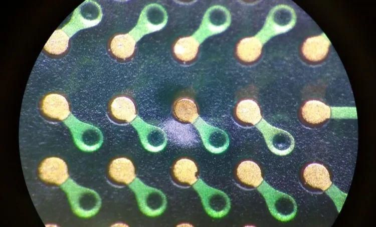
A pass hole is a hole on the circuit board that connects two or more layers. In general, the hole transmits the signal carried by the circuit from one layer of the board to the corresponding circuit on the other layer. In order to conduct signals between the wiring layers, the holes are metallized during the manufacturing process. According to the specific use, the size of the hole and the pad are different. Smaller through-holes are used for signal wiring, while larger through-holes are used for power and ground wiring, or to help heat overheating devices.
Different types of holes on the circuit board
through-hole
The through-hole is the standard through-hole that has been used on double-sided printed circuit boards since they were first introduced. The holes are mechanically drilled through the entire circuit board and are electroplated. However, the minimum bore that can be drilled by a mechanical drill has certain limitations, depending on the aspect ratio of the drill diameter to the plate thickness. Generally speaking, the aperture of the through hole is not less than 0.15 mm.
Blind hole:
Like through-holes, the holes are drilled mechanically, but with more manufacturing steps, only part of the plate is drilled from the surface. Blind holes also face the problem of bit size limitation; But depending on which side of the board we are on, we can wire above or below the blind hole.
Buried hole:
Buried holes, like blind holes, are drilled mechanically, but start and end in the inner layer of the board rather than the surface. This through-hole also requires additional manufacturing steps due to the need to be embedded in the plate stack.
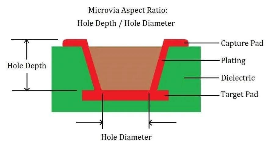
Micropore
This perforation is ablated with a laser and the aperture is less than the 0.15 mm limit of a mechanical drill bit. Because the microholes span only two adjacent layers of the board, the aspect ratio makes the holes available for plating much smaller. Microholes can also be placed on the surface or inside of the board. The microholes are usually filled and plated, essentially hidden, and can therefore be placed in surface-mount element solder balls of components such as ball grid arrays (BGA). Due to the small aperture, the pad required for the microhole is also much smaller than the ordinary hole, about 0.300 mm.
According to the design requirements, the above different types of holes can be configured to make them work together. For example, micropores can be stacked with other micropores, as well as with buried holes. These holes can also be staggered. As mentioned earlier, microholes can be placed in pads with surface-mount element pins. The problem of wiring congestion is further alleviated by the absence of the traditional routing from the surface mount pad to the fan outlet.