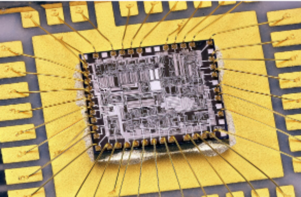
Wire bonding – the method of mounting a chip onto a PCB
There are 500 to 1,200 chips connected to each wafer before the end of the process. In order to use these chips where needed, the wafer needs to be cut into individual chips and then connected to the outside and powered on. At this time, the method of connecting wires (transmission paths for electrical signals) is called wire bonding.
Material of wirebonding: gold /aluminum /copper
Material of wirebonding is determined by comprehensively considering various welding parameters and combining them into the most appropriate method. The parameters referred to here involve many matters, including semiconductor product type, packaging type, pad size, metal lead diameter, welding method, as well as reliability indicators such as the tensile strength and elongation of the metal lead. Typical metal lead materials include gold, aluminum and copper. Among them, gold wire is mostly used for semiconductor packaging.
Gold Wire has good electrical conductivity, is chemically stable, and has strong corrosion resistance. However, the biggest disadvantage of aluminum wire, which was mostly used in the early days, was that it was easy to corrode. Moreover, the hardness of the gold wire is strong, so it can be well formed into a ball in the primary bonding, and can properly form a semicircular lead loop (Loop, from primary bonding to secondary bonding) in the secondary bonding. the shape formed).
Aluminum Wire has a larger diameter and larger pitch than gold wire. Therefore, even if high-purity gold wire is used to form the lead loop, it will not break, but pure aluminum wire will break easily, so it will be mixed with some silicon or magnesium to make an alloy. Aluminum wire is mainly used in high-temperature packaging (such as Hermetic) or ultrasonic methods where gold wire cannot be used.
Although copper wire is cheap, its hardness is too high. If the hardness is too high, it will not be easy to form into a ball shape, and there are many limitations when forming lead loops. Moreover, pressure must be applied to the chip pad during the ball bonding process. If the hardness is too high, cracks will appear in the film at the bottom of the pad. In addition, there will be a “peeling” phenomenon in which the firmly connected pad layer peels off. Nevertheless, since the metal wiring of the chip is made of copper, there is an increasing trend to use copper wire nowadays. Of course, in order to overcome the shortcomings of copper wire, it is usually mixed with a small amount of other materials to form an alloy and then used.