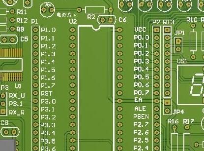
Flexible Printed Circuit
Flexible Printed Circuit,It can be bent, wound and folded freely. The flexible circuit board is processed by using polyimide film as the base material. It is also called soft board or FPC in the industry. The process flow of flexible circuit board is divided into Double-sided flexible circuit board process, multi-layer flexible circuit board process. The FPC soft board can withstand millions of dynamic bending without damaging the wires. It can be arranged arbitrarily according to the requirements of the space layout, and can be moved and stretched arbitrarily in the three-dimensional space, so as to achieve the integration of component assembly and wire connection; the flexible circuit board can be The size and weight of electronic products are greatly reduced, and it is suitable for the development of electronic products in the direction of high density, miniaturization and high reliability.
The structure of flexible boards: according to the number of layers of conductive copper foil, it can be divided into single-layer boards, double-layer boards, multi-layer boards, double-sided boards, etc.
Material properties and selection methods:
(1) Substrate: The material is polyimide (POLYMIDE), which is a high temperature resistant, high strength polymer material. It can withstand the temperature of 400 degrees Celsius for 10 seconds, and the tensile strength is 15,000-30,000PSI. 25μm thick substrates are the cheapest and most widely used. If the circuit board is required to be harder, a substrate of 50 μm should be used. Conversely, if the circuit board needs to be softer, use a 13μm substrate
(2) Transparent glue for the base material: It is divided into two types: epoxy resin and polyethylene, both of which are thermosetting glue. The strength of polyethylene is relatively low. If you want the circuit board to be soft, choose polyethylene. The thicker the substrate and the clear glue on it, the stiffer the board. If the circuit board has a relatively large bending area, you should try to use a thinner substrate and transparent glue to reduce the stress on the surface of the copper foil, so that the chance of micro-cracks in the copper foil is relatively small. Of course, for such areas, single-layer boards should be used as much as possible.
(3) Copper foil: divided into rolled copper and electrolytic copper. Rolled copper has high strength and is resistant to bending, but it is more expensive. Electrolytic copper is much cheaper, but its strength is poor and it is easy to break. It is generally used in occasions where there is little bending. The choice of copper foil thickness depends on the minimum width and minimum spacing of the leads. The thinner the copper foil, the smaller the minimum achievable width and spacing. When choosing rolled copper, pay attention to the rolling direction of the copper foil. The rolling direction of the copper foil should be consistent with the main bending direction of the circuit board.
(4) Protective film and its transparent glue: A protective film of 25 μm will make the circuit board harder, but the price is cheaper. For circuit boards with relatively large bends, it is best to use a 13μm protective film. Transparent glue is also divided into two types: epoxy resin and polyethylene. The circuit board using epoxy resin is relatively hard. After the hot pressing is completed, some transparent glue will be extruded from the edge of the protective film. If the size of the pad is larger than the opening size of the protective film, the extruded glue will reduce the size of the pad and cause its edge to be irregular. At this time, try to use transparent glue with a thickness of 13 μm.
(5) Pad plating: For circuit boards with relatively large bends and some exposed pads, electroplating nickel + chemical gold plating should be used, and the nickel layer should be as thin as possible: 0.5-2μm, chemical gold layer 0.05-0.1 μm.
