News
-
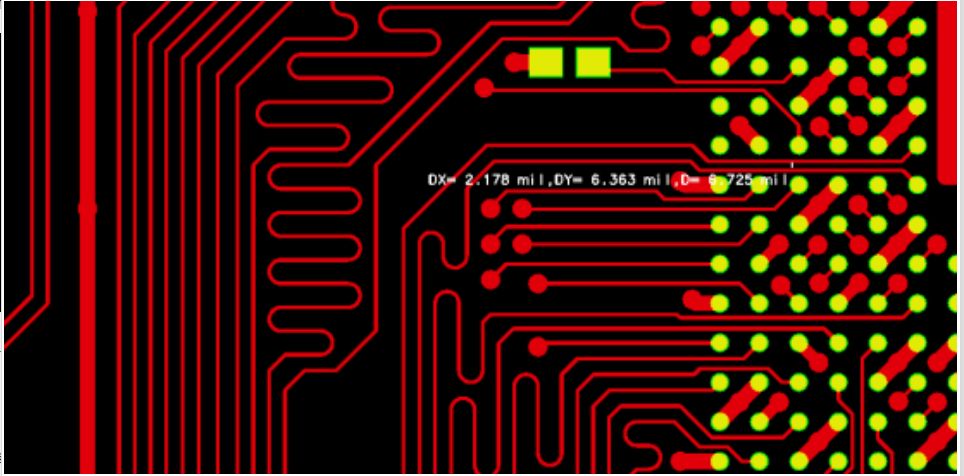
DFM design of PCB manufacturing spacing
The electrical safety spacing mainly depends on the level of the plate-making factory, which is generally 0.15mm. In fact, it can be even closer. If the circuit is not related to the signal, as long as there is no short circuit and the current is sufficient, large current requires thicker wiring ...Read more -
Several Inspection Methods of PCBA Board Short Circuit
In the process of SMT chip processing, short circuit is a very common poor processing phenomenon. The short circuited PCBA circuit board cannot be used normally. The following is a common inspection method for short circuit of PCBA board. 1. It is recommended to use a short circuit positi...Read more -
Manufacturability design of PCB electrical safety distance
There are many PCB design rules. The following is an example of electrical safety spacing. Electrical rule setting is the design circuit board in the wiring must abide by the rules, including the safety distance, open circuit, short circuit setting. The setting of these parameters will affect the...Read more -
Ten defects of PCB circuit board design process
PCB circuit boards are widely used in various electronic products in today’s industrially developed world. According to different industries, the color, shape, size, layer, and material of PCB circuit boards are different. Therefore, clear information is required in the design of PCB circui...Read more -
What is the PCB warpage’s standard?
In fact, PCB warping also refers to the bending of the circuit board, which refers to the original flat circuit board. When placed on the desktop, the two ends or the middle of the board appear slightly upward. This phenomenon is known as PCB warping in the industry. The formula for calculating t...Read more -
What are the requirements of laser welding process for PCBA design?
1.Design for Manufacturability of PCBA The manufacturability design of PCBA mainly solves the problem of assemblability, and the purpose is to achieve the shortest process path, the highest soldering pass rate, and the lowest production cost. The design content mainly includes: ...Read more -
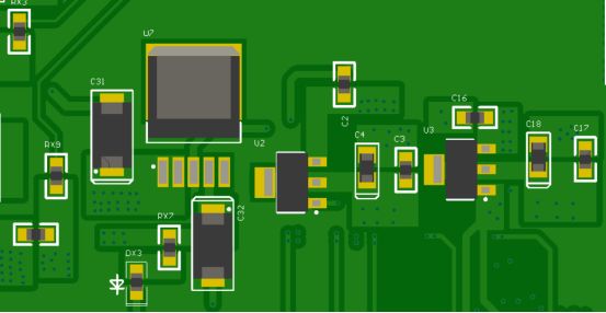
Manufacturability design of PCB layout and wiring
Regarding the PCB layout and wiring problem, today we will not talk about signal integrity analysis (SI), electromagnetic compatibility analysis (EMC), power integrity analysis (PI). Just talking about the manufacturability analysis (DFM), the unreasonable design of manufacturability will also le...Read more -
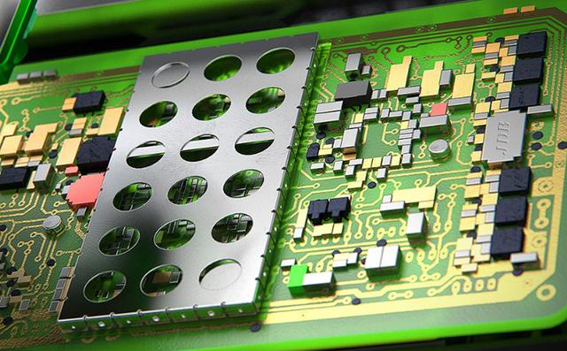
SMT processing
SMT processing is a series of process technology for processing on the basis of PCB. It has the advantages of high mounting accuracy and fast speed, so it has been adopted by many electronic manufacturers. The SMT chip processing process mainly includes silk screen or glue dispensing, mounting or...Read more -
How to make a good PCB board?
We all know that making PCB board is to turn the designed schematic into a real PCB board. Please don’t underestimate this process. There are many things that are feasible in principle but difficult to achieve in the project, or others can achieve things that some people can not achieve Moo...Read more -
How to design PCB crystal oscillator?
We often compare the crystal oscillator to the heart of the digital circuit, because all the work of the digital circuit is inseparable from the clock signal, and the crystal oscillator directly controls the whole system. If the crystal oscillator does not operate, the whole system will be paraly...Read more -
Analysis of three kinds of PCB stencil technology
According to the process, the pcb stencil can be divided into the following categories: 1. Solder paste stencil: As the name suggests, it is used to brush solder paste. Carve holes in a piece of steel that correspond to the pads of the pcb board. Then use solder paste to pad to the PCB board thr...Read more -
Ceramic PCB circuit board
Advantage: Large current carrying capacity, 100A current continuously passes through the 1mm0.3mm thick copper body, the temperature rise is about 17℃; 100A current continuously passes through the 2mm0.3mm thick copper body, the temperature rise is only about 5℃. Better heat dissipation performan...Read more


