Introduction of Via-in-Pad:
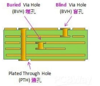
It is well known that vias (VIA) can be divided into plated through hole, blind vias hole and buried vias hole, which have different functions.
With the development of electronic products, vias play a vital role in the interlayer interconnection of printed circuit boards. Via-in-Pad is widely used in small PCB and BGA (Ball Grid Array). With the inevitable development of high density, BGA (Ball Grid Array) and SMD chip miniaturization, the application of Via-in-Pad technology is becoming more and more important.
Vias in pads have many advantages over blind and buried vias:
. Suitable for fine pitch BGA.
. It is convenient to design higher density PCB and save wiring space.
. Better thermal management.
. Anti-low inductance and other high-speed design.
. Provides a flatter surface for components.
. Reduce PCB area and further improve wiring.
Due to these advantages, via-in-pad is widely used in small PCBs, especially in PCB designs where heat transfer and high speed are required with limited BGA pitch. Although blind and buried vias help increase density and save space on PCBs, vias in pads are still the best choice for thermal management and high-speed design components.
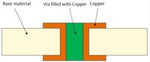
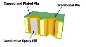
With a reliable via filling/plating capping process, via-in-pad technology can be used to produce high-density PCBs without using chemical housings and avoiding soldering errors. In addition, this can provide additional connecting wires for BGA designs.
There are various filling materials for the hole in the plate, silver paste and copper paste are commonly used for conductive materials, and resin is commonly used for non-conductive materials